


 19 / 66

C
opper-niobium nanolaminates,
composed of alternating layers of
Cu and Nb, display high strengths
(>1 GPa) and intriguing properties due to
their highly oriented nanocrystalline mi-
crostructure. Compared to either pure Cu
or Nb, these composite materials have
superior hardness, flow strength, and
radiation damage resistance
[1-2]
. While
nanolaminates were previously only
available in thin-film form (<40 µmthick),
recent advances in the severe plastic de-
formation process of accumulative roll
bonding (ARB) have enabled production
of bulk nanolaminates (Fig. 1). Four-mm
thick Cu-Nb nanolaminates containing
more than 200,000 individual layers (lay-
er thickness of <20 nm) are now routinely
synthesized for research purposes.
The ability to produce bulk metal-
lic nanolaminates has greatly expanded
the potential structural applications for
these materials, motivating investi-
gations into formability, joining tech-
niques, and deformation behavior. This
article presents an overview of both the
ARB process and the materials’ defor-
mation behavior.
Synthesismethod
The ARB process uses an iterative
sequence of cleaning, stacking, cold roll
bonding, and cutting to create and re-
fine a lamellar microstructure. Starting
materials consist of coarse-grained sin-
gle-phase sheets of Cu and Nb which are
degreased, wirebrushed, and alternately
stacked. Materials are bonded together
using a single-pass 50% rolling reduc-
tion. Next, the roll bonded sheet is cut
in half, cleaned, and re-stacked in prepa-
ration for the next cycle. Iterating these
steps increases the number of layers ex-
ponentially while decreasing layer thick-
ness (Fig. 2). Sheet thicknesses remain
nearly constant during process-
ing, and can be increased by
cutting and bonding three or
more pieces together.
This processing technique
allows extreme strains to be
imparted to the material while
maintaining the desired sheet
thickness. Strains exceed those
typically encountered during
conventional rolling. For exam-
ple, synthesis of 15 nm Cu-Nb
nanolaminates requires a roll-
ing strain of 11.8. Imagine a U.S.
nickel coin (nearly the same
thicknesses as the sheets used
for ARB). If it were convention-
ally rolled to a strain of 11.8, the
length of the rolled strip would
exceed 2 km.
While ARB has been ap-
plied to several different bimet-
al systems
[3-5]
, the Cu-Nb sys-
tem offers low solid solubility
as well as similar flow stresses
for the two phases. These char-
acteristics result in excellent
microstructural stability during
ARB processing, allowing pro-
duction of nanolaminates with
continuous layers and individu-
al layer thicknesses as small as
10 nm
[6]
.
Deformation
behavior
The large dimensions of ARB Cu-Nb
nanolaminates have facilitated a wide
variety of bulk mechanical tests (i.e., ten-
sile tests, miniature Charpy impact tests,
and fatigue tests) that are difficult, if not
impossible, to performon traditional thin
filmnanolaminates. Inmany cases, these
tests confirm the extraordinary proper-
ties of metallic nanolaminates. For ex-
ample, tensile specimens of ARB Cu-Nb
nanolaminates with a 30 nm layer thick-
ness have a strain-to-failure of approx-
imately 8% and a flow strength of 1200
MPa (a 5× increase in strength compared
to pure Cu or Nb)
[7]
. However, bulk me-
chanical testing also reveals an unusual
deformationmode during compression.
During layer-parallel compression
of nanolaminate specimens with layer
thicknesses below100 nm, apronounced
inhomogeneous shape change occurs
A D V A N C E D
M A T E R I A L S
&
P R O C E S S E S | F E B R U A R Y
2 0 1 5
1 9
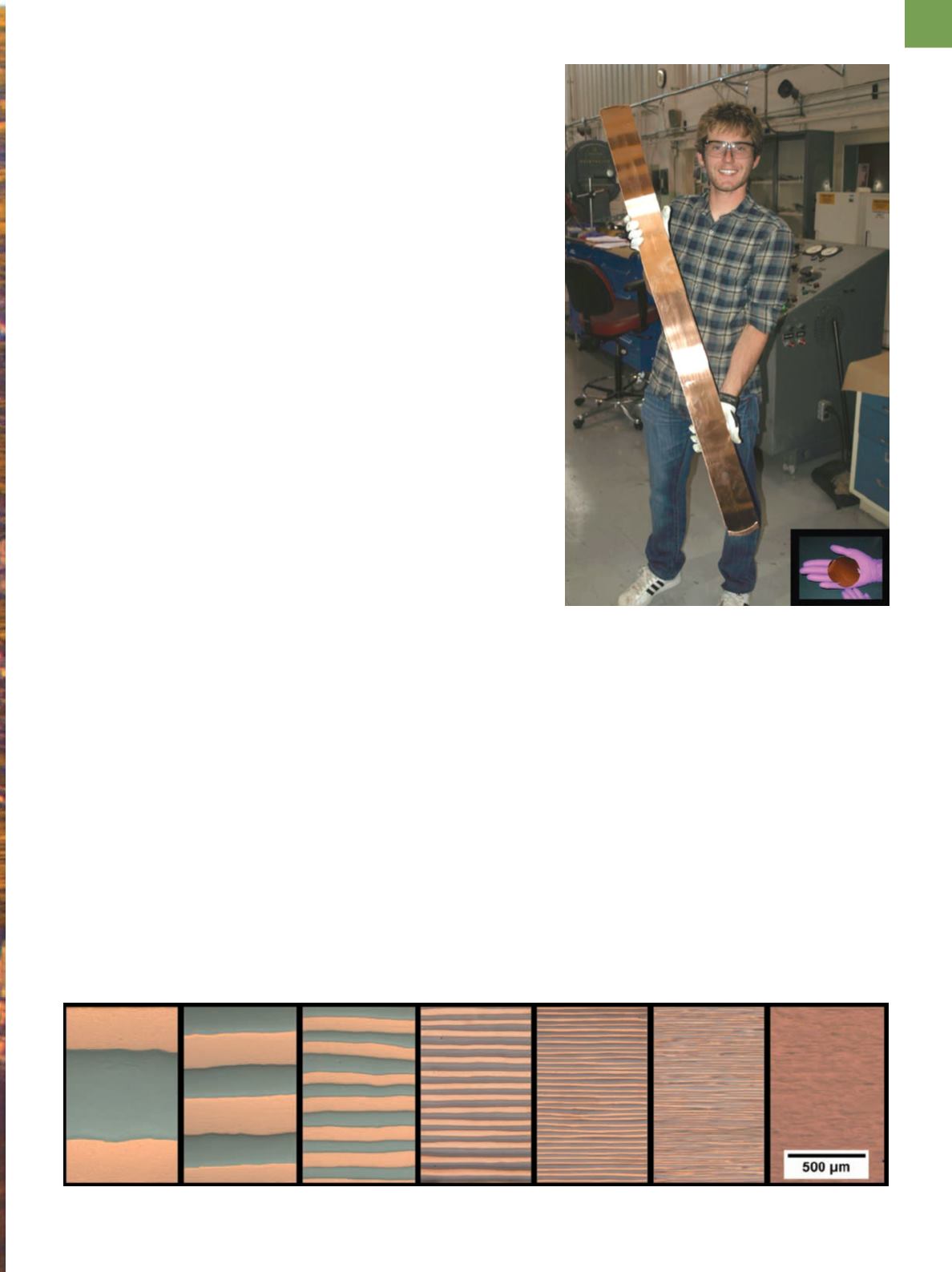
Fig. 1
— A 4-mm-thick piece of Cu-Nb nanolaminate
material synthesized using the ARB process held by
Thomas Nizolek. For comparison, a thin-film Cu-Nb
multilayer synthesized using physical vapor
deposition is shown in the bottom right.
Fig. 2
—Optical micrographs show cross-sections of Cu-Nb laminates at various stages during the ARB process.