



 45 / 58

edfas.org
45
ELECTRONIC DEVICE FAILURE ANALYSIS | VOLUME 19 NO. 2
ENGINEERS SHRINK MICROSCOPE TO
DIME-SIZED DEVICE
Researchers at The University of Texas at Dallas (Rich-
ardson, Texas) have created an atomic force microscope
(AFM) on a chip, dramatically shrinking the size—and,
hopefully, the price tag—of a high-tech device commonly
used to characterize material properties.
“A standard AFM is a large, bulky instrument, with
multiple control loops, electronics, and amplifiers,” said
Dr. RezaMoheimani, professor of mechanical engineering
at UT Dallas. “We have managed to miniaturize all of the
electromechanical components onto a single small chip.”
Moheimani and his colleagues describe their proto-
type device in the article “On-Chip Dynamic Mode Atomic
ForceMicroscopy: ASilicon-on-InsulatorMEMSApproach,”
published in the February 2017 issue of the
IEEE
Journal
of Microelectromechanical Systems
.
AnAFM is a scientific tool that is used to create detailed
three-dimensional images of the surfaces of materials,
down to the nanometer scale—that’s roughly on the scale
of individual molecules.
The basic AFM design consists of a tiny cantilever,
or arm, that has a sharp tip attached to one end. As the
apparatus scans back and forth across the surface of a
sample, or the sample moves under it, the interactive
forces between the sample and the tip cause the cantilever
to move up and down as the tip follows the contours of
the surface. Those movements are then translated into
an image.
“An AFM is a microscope that ‘sees’ a surface kind of
the way a visually impaired person might, by touching.
You can get a resolution that is well beyond what an
optical microscope can achieve,” said Moheimani, who
holds the James Von Ehr Distinguished Chair in Science
and Technology in the Erik Jonsson School of Engineering
and Computer Science. “It can capture features that are
very, very small.”
The UT Dallas team created its prototype on-chip
AFM using a microelectromechanical systems (MEMS)
approach.
“A classic example of MEMS technology is the accel-
erometers and gyroscopes found in smartphones,” said
Dr. Anthony Fowler, a research scientist in Moheimani’s
Laboratory for Dynamics and Control of Nanosystems
and one of the article’s co-authors. “These used to be big,
expensive mechanical devices, but using MEMS technol-
ogy, accelerometers have shrunk down onto a single chip,
which can bemanufactured for just a few dollars apiece.”
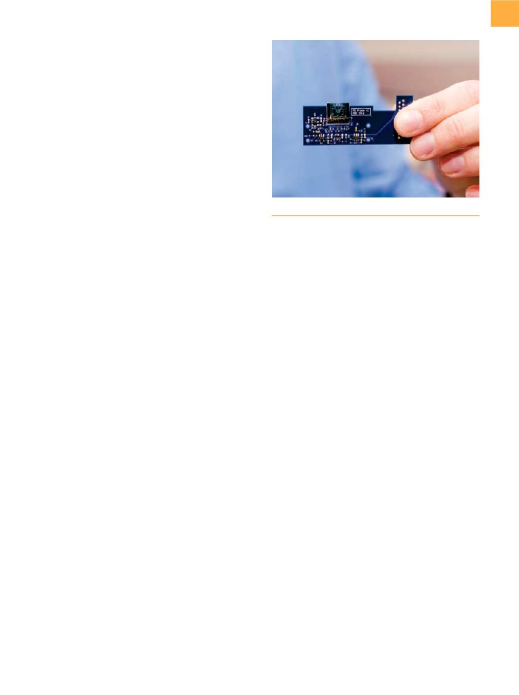
The MEMS-based AFM is approximately 1 cm
2
in size,
or a little smaller than a dime. It is attached to a small
printed circuit board, approximately half the size of a
credit card, which contains circuitry, sensors, and other
miniaturized components that control themovement and
other aspects of the device.
Conventional AFMs operate in various modes. Some
map out a sample’s features by maintaining a constant
forceas theprobe tipdrags across the surface, whileothers
do so by maintaining a constant distance between the
two. “The problemwith using a constant-height approach
is that the tip is applying varying forces on a sample all
the time, which can damage a sample that is very soft,”
Fowler said. “Or, if you are scanning a very hard surface,
you could wear down the tip.”
TheMEMS-basedAFMoperates in tappingmode,which
means the cantilever and tip oscillate up and down per-
pendicular to the sample, and the tip alternately contacts
and then lifts off from the surface. As the probe moves
back and forth across a sample material, a feedback
loop maintains the height of that oscillation, ultimately
creating an image.
“In tapping mode, as the oscillating cantilever moves
across the surface topography, the amplitude of the oscil-
lation wants to change as it interacts with the sample,”
said Dr. Mohammad Maroufi, a research associate in
mechanical engineering and co-author of the paper. “This
device creates an image by maintaining the amplitude of
oscillation.”
Because conventional AFMs require lasers and other
large components to operate, their use can be limited.
They are also expensive. “An educational version can
cost about $30,000 or $40,000, and a laboratory-level AFM
can run $500,000 or more,” Moheimani said. “Our MEMS
MEMS-based AFM attached to a small printed circuit board