
edfas.org
25
ELECTRONIC DEVICE FAILURE ANALYSIS | VOLUME 18 NO. 3
• “Scanning Acoustic GHz-Microscopy versus
Conventional SAM for Advanced Assessment of Ball
Bond and Metal Interfaces in Microelectronic Devices”
• “New I.R. Thermography Methodology for Failure
Analysis on Tantalum Capacitors”
• Comprehensive 2-D Carrier Profiling of Low Doping
Region by High-Sensitivity Scanning Spreading
Resistance Microscopy (SSRM) for Power Device
Applications”
• “Unsupervised Learning for Signal Mapping inDynamic
Photon Emission”
• “Useof aSiliconDriftDetector forCathodoluminescence
Detection”
• “Failure Analysis on Recovering Low Resistive Via in
Mixed-Mode Device”
• “RF Functional-Based Complete FA Flow”
• “Improvement of Signal-to-Noise Ratio in Electro-
Optical Probing Technique by Wavelets Filtering”
• “Visualization of Gate-Bias-Dependent Carrier
Distribution in SiCPower-MOSFETUsing Super-Higher-
Order Scanning Nonlinear Dielectric Microscopy”
• “Electrical Model of an Inverter Body Biased Structure
in Triple-Well Technology under Pulsed Photoelectric
Laser Stimulation”
• “DieCrackFailureMechanismInvestigationsDepending
on the Time of Failure”
• “Latent Gate Oxide Defects Case Studies”
• “Top-Down Delayering to Expose Large Inspection
Area on Die Side-Edge with Platinum (Pt) Deposition
Technique”
• “Auger Electron Spectroscopy Characterization of
Ti/NiV/Ag Multilayer Back-Metal for Monitoring of Ni
Migration on Ag Surface”
• “Magnetic Imaging for Resistive, Capacitive, and
Inductive Devices: From Theory to Piezo Actuator
Failure Localization”
• “Microscopic Investigation of SiO
2
/SiC Interface Using
Super-Higher-Order Scanning Nonlinear Dielectric
Microscopy”
• “Thermoreflectance Mapping Observation of Power
MOSFET under UIS Avalanche Breakdown Condition”
• “Characteristics and Early Failure of PCB Embedded
Power Electronics”
• “Fault Isolation in a Case Study of Failure Analysis on
Metal-Insulator-Metal Capacitor Structures”
• “High-Resolution X-Ray Computed Tomography of
Through-Silicon Vias for RF MEMS Integrated Passive
Device Applications”
• “Compact Thermal Modeling of Spin Transfer Torque
Magnetic Tunnel Junction”
The failure analysis track also had three embedded
workshops:
• Advanced tools and techniques flash presentations:
mini-workshops on methods and tools for failure
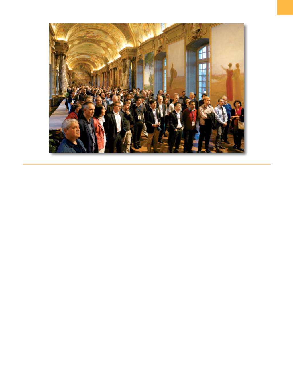
Cocktails in the Salle des Illustres at Capitole, the Toulouse city hall


