


 12 / 102

A D V A N C E D M A T E R I A L S & P R O C E S S E S | O C T O B E R 2 0 1 5
1 2
TESTING | CHARACTERIZATION
OPTICAL LENSES MADE
OF NANOPILLARS
A team of researchers recently
developed flat optical lenses as part
of a collaboration between NASA’s Jet
Propulsion Laboratory and the Cali-
fornia Institute of Technology, both in
Pasadena. These optical components
are capable of manipulating light in
ways that are difficult or impossible
to achieve with conventional optical
devices. The new lenses are not made
of glass. Instead, silicon nanopillars are
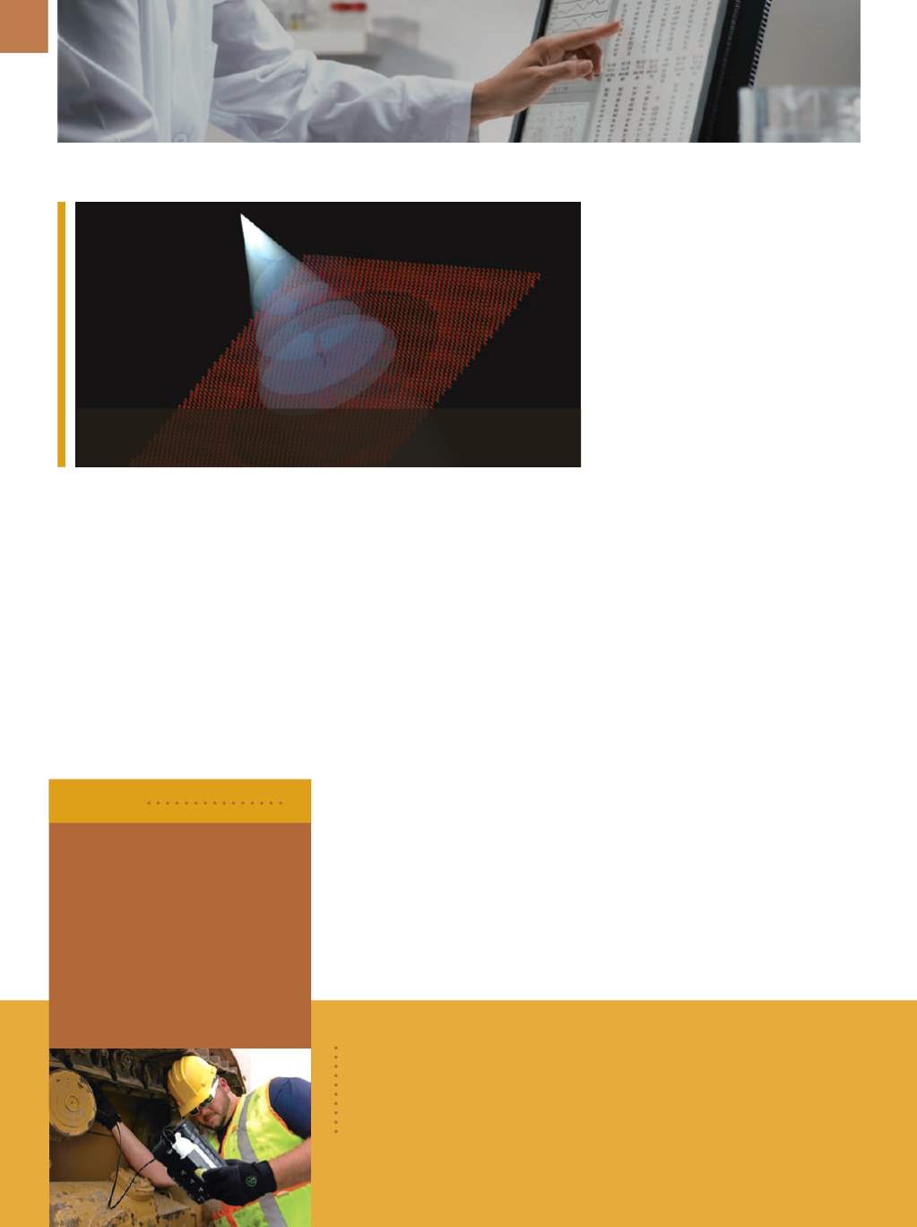
Schematic shows how a metasurface can generate and focus radially polarized light.
Courtesy of Amir Arbabi/Faraon Lab/Caltech.
of each pillar and rotating them around
their axes, scientists were able to simul-
taneously manipulate the phase and
polarization of passing light. In addi-
tion, the new lenses can be used to
modify the shape of light beams at will.
Semiconductor lasers typically emit
into elliptical beams that are difficult
to work with, and the new metasur-
face optical components could replace
expensive optical systems used to circu-
larize the beams. The team is currently
working with industrial partners to cre-
ate metasurfaces for use in commer-
cial devices such as miniature cameras
and spectrometers, although a limited
number are now being used in optical
experiments by collaborating scientists
in other disciplines.
jpl.nasa.gov.ULTRAFAST ELECTRON
DIFFRACTION RESEARCH
SPEEDS AHEAD
A new instrument at the DOE’s
SLAC National Accelerator Labora-
tory, Menlo Park, Calif., uses a method
known as ultrafast electron diffraction
(UED) to reveal motions of electrons
and atomic nuclei within molecules
that take place in less than a tenth of
a trillionth of a second. The technique
complements ultrafast studies with
SLAC’s x-ray free-electron laser. Similar
to x-ray light, highly energetic electrons
can take snapshots of the interior of
materials as they pass through them.
Yet electrons interact differently with
materials and “see” different things.
Combining both methods enables a
arranged into a honeycomb pattern to
create a metasurface that can control
the paths and properties of passing light
waves. Applications include advanced
microscopes, displays, sensors, and
cameras that can be mass-produced
using the same techniques used to
manufacture computer chips.
“Currently, optical systems are
made one component at a time, and
the components are often manually
assembled,” says Andrei Faraon, assis-
tant professor of applied physics and
materials science at Caltech. “But this
new technology is very similar to the
one used to print semiconductor chips
onto silicon wafers, so you could con-
ceivably manufacture millions of micro-
scopes or cameras at a time.”
Seen under a scanning electron
microscope, the new metasurfaces
resemble a cut forest where only the
stumps remain. Each silicon stump, or
pillar, has an elliptical cross-section,
and by carefully varying the diameters
Modustri,
Grand Rapids, Mich.,
entered into a strategic alliance
with
Caterpillar Inc.
(Cat), Peo-
ria, Ill. The companies will work
together to enhance the abilities of
Cat’s customers to measure wear
on parts in new ways, potential-
ly saving hundreds of hours and
millions of dollars in maintenance
expenses.
modustri.com.
BRIEFS
Nordson Corp.,
Westlake, Ohio, acquired
MatriX Technologies GmbH,
Munich, a manufacturer of automated x-ray inspection equipment used
to ensure the quality of electronic printed circuit boards, critical electron-
ic devices, and fully assembled products in consumer, automotive, and
other industrial markets.
nordson.com.