


 12 / 70

Copper-oxide material aids understanding of superconductivity
A new study by scientists at the
Max Planck Institute for the Structure
and Dynamics of Matter in Germany
and the U.S. Dept. of Energy’s SLAC
and Brookhaven national laboratories
pins down a major factor behind the
appearance of superconductivity in a
promising copper-oxide material.
Carefully timed pairs of laser pulses at
SLAC National Accelerator Labora-
tory’s Linac Coherent Light Source
(LCLS) were used to trigger super-
conductivity in the material and im-
mediately take x-ray snapshots of its
atomic and electronic structure as su-
perconductivity emerged.
So-called “charge stripes” of increased electrical charge melt away as superconductiv-
ity appears. These results help rule out the theory that shifts in the material’s atomic lat-
tice hinder the onset of superconductivity. Based on this new understanding, scientists
may be able to develop techniques to eliminate charge stripes and help pave the way for
room-temperature superconductivity, often considered the holy grail of condensed matter
physics. The demonstrated ability to rapidly switch between insulating and superconduct-
ing states could also prove useful in advanced electronics and computation.
“The very short timescales and the need for high spatial resolution made this experi-
ment extraordinarily challenging,” explains Michael Först, a scientist at the Max Planck In-
stitute. “Using femtosecond x-ray pulses, we captured the quadrillionths-of-a-second
dynamics of the charges and the crystal lattice. We’ve broken new ground in understand-
ing light-induced superconductivity.”
The compound used in this study was a layered material consisting of lanthanum, bar-
ium, copper, and oxygen grown at Brookhaven Lab by physicist Genda Gu. Each copper
oxide layer contained the crucial charge stripes.
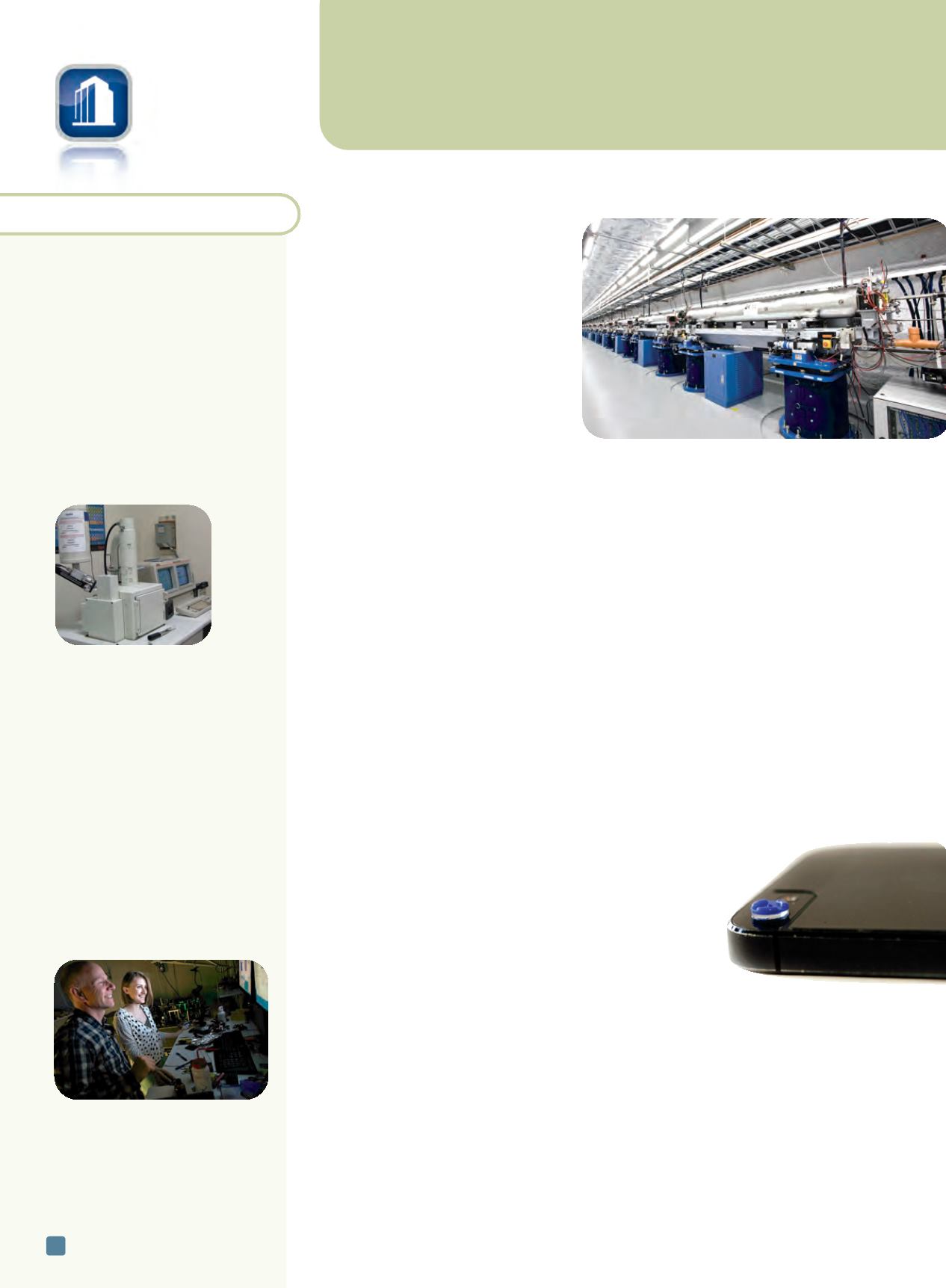
www.bnl.gov.Adhesive-free lens turns smartphones into microscopes
A new device called the Micro Phone Lens, developed by University
of Washington (UW) mechanical engineering alumnus Thomas Lar-
son, turns any smartphone or tablet into a handheld microscope.
The pliable lens sticks to a device’s camera without any adhe-
sive and makes it possible to see things magnified dozens of
times on the screen. Larson graduated in 2013 and formed his
own company in Olympia, Wash.
The lens is about the size of a button and comes in its own
carrying case. It sticks flat onto smartphone camera lenses, then an
external light source such as a lamp is turned on, and the device is
run in camera mode. Moving the device closer or farther from the
object brings it into focus. Several other products exist that can
adapt a smartphone to be used as a microscope, but they are signif-
icantly more expensive and the attachments are heavy or require
permanent adhesives.
Larson developed his lens while working in the lab of Nathan Sniadecki, UW associate
professor of mechanical engineering. Larson’s lens is now as powerful as the research mi-
croscopes used in the lab, says Sniadecki. After graduation, Larson ran a Kickstarter cam-
paign for the 15X microscope lens, and more than 5000 people signed up. He shipped
orders to people around the world who need microscopes they can use in the field or in
briefs
Durex Industries,
Cary, Ill.,
expanded its testing and analysis
capabilities into a new 2000-sq-ft
metrology laboratory and added a
scanning electron microscope
(SEM). Services at the new lab
include microstructural analysis
such as grain size measurement,
inclusion level, and weld
penetration; SEM imaging; EDS
elemental composition analysis;
thermal imaging (FLIR); x-ray
imaging; finite element analysis;
and micro-hardness analysis.
www.durexindustries.com.
Durex Industries’ new
metrology lab.
A team of
Harvard University
scientists, Cambridge, Mass., led
by physics professor
Amir Yacoby,
developed a magnetic resonance
imaging (MRI) system that can
produce nanoscale images.
Though not yet precise enough to
capture atomic-scale images of a
single molecule, the system has
already captured images of single
electron spins. As the system is
refined, Yacoby expects it to
eventually be precise enough to
peer into the structure of individual
molecules.
www.harvarduniversity.edu.
Physics professor Amir Yacoby
and research assistant Yuliya
Dovzhenko work in the lab where
an MRI system that can produce
nanoscale images was
developed. Courtesy of Kris
Snibbe/Harvard.
ADVANCED MATERIALS & PROCESSES •
MAY 2014
12
T
ESTING
C
HARACTERIZATION
news
industry
The Undulator Hall of SLAC Lab’s Linac Coherent
Light Source, which “wiggles” electrons to generate
high-power coherent x-rays crucial to studying
superconductivity.
A new lens that
sticks to a device’s
camera without
using adhesive can
turn any smart-
phone or tablet into
a handheld
microscope.